Image
Interconnect technology based on organic materials
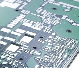
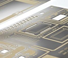
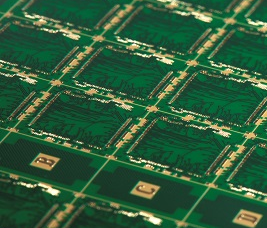
We offer every type of leading-edge PCBs and organic substrates with the highest degree of commitment and flexibility. Full traceability is guaranteed from the lot level down to the individual print on a panel as well as for all base materials.
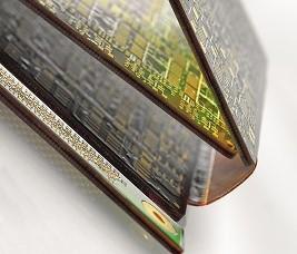
- Ultra-HDI multilayer flex PCBs
- Ultra-thin materials
- Ultra-fine line cables
- 3D miniaturization
- Filled and stacked microvias
- Buried, blind, staggered and stacked vias
- Multilayer full flex material
- 3D miniaturization by folding
- Small bend zones in multiple shapes
- Combination of PI and LCP fley possible
- Microvia and ultra-fine line technology
- Reduced overall thickness
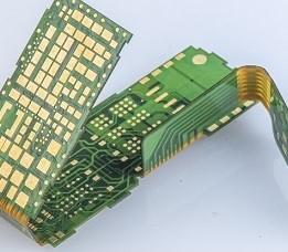
- Ultra-HDI multilayer rigid-flex PCBs
- High-grade 3D miniaturization
- Sequential and parallel build-ups
- Versatile combinations of base materials
- Thinned bending zones
- Book binder build-ups
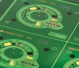
- Ultra-HDI multilayer rigid build-ups
- Buried, blind, staggered and stacked vias
- Profiles, cavities, cut-outs and castellations
- Low CTE materials
- Thermal management solutions
- Constraining materials such as CIC, CMC, CCC
- Very flexible thermoplast
- Near hermetic due to very low water absorption
- Temperature stable up to 190°C
- Low weight
- Excellent high frequency properties
- Fully biocompatible base material
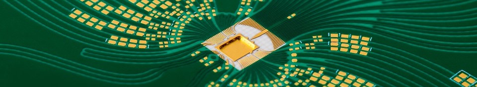
- Substrates for SDBGAs, CSPs, SiPs and MCMs
- Ultra-thin materials for light-weight build-ups
- Stacked vias and via-in-pad
- High density pitch design
- Die cavities
- Anylayer or HDI technology