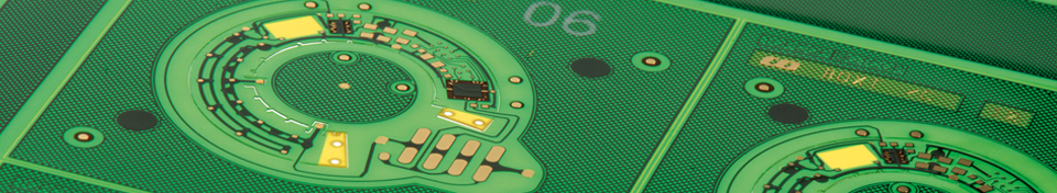
HDI & Ultra-HDI Flex Printed Circuits
Flex Printed Circuits (FPC) are gaining ground due to their distinct advantages for multiple applications. Continuous miniaturization, ever-increasing cost pressure and the attempts to reduce weight and space consumption while at the same time increasing the level of integration are some of the drivers for the utilization of FPCs.
Dyconex has its distinct history in driving technologies and applications for FPC in various business fields and is used to meet your cutting-edge design requirements while fulfilling the most demanding quality standards of medical and defense industries at the same time.
Definitions:
1) HDI flex – L/S 50-150 µm, via 75-150 µm
2) Ultra-HDI flex – L/S <50 µm, via < 75 µm
Technology Highlights
- Turnkey flex solutions targeting 3D miniaturization
- Highly reliable, extremely robust multilayer flex/microvia substrates
- Ultra-thin base materials
- Filled via and stacked via process available
- Complex mechanical/assembly assist features, including special profiles, fold lines, cut-outs and thinned bending zones/cavities
- Wrap-around boards
- Chip-on-flex (COF), chip scale packaging (CSP) substrates, and BGAs
- A wide variety of surface finishes, for example OSP, ENIG, ENEPIG, E-AU, DIG
- Flying leads
- Bending test for flexible circuits
- Ultra-fine line flex cables
General capabilities for flex circuit boards:
|
Description |
Standard Capability |
|
Lines/spaces |
25/35 µm |
|
Microvias/pads diameter |
50/150 µm |
|
Thinnest starting material |
25 µm |
|
Thinnest dielectric thickness |
12 µm |
|
Conductor width tolerance |
+/- 20% |
|
Artwork to soldermask tolerance |
+/- 25 µm |
|
Layer count |
8 |
|
Description |
Leading edge capability |
|
Lines/spaces |
20/25 µm |
|
Microvias/pads diameter |
40/100 µm |
|
Thinnest starting material |
12 µm |
|
Thinnest dielectric thickness |
5 µm |
|
Conductor width tolerance |
+/- 10 % |
|
Artwork to soldermask tolerance |
+/- 15 µm |
|
Layer count |
10+ |