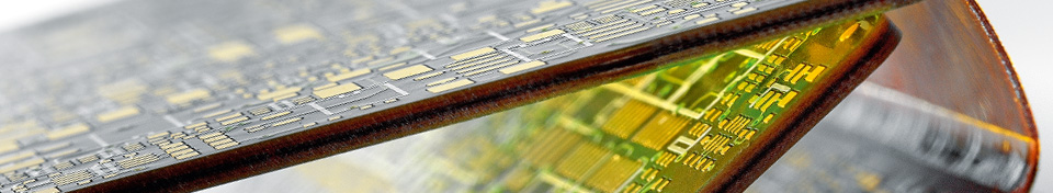
Rigid-Flex
In some applications Printed Circuit Boards (PCB) may need flexibility for a space saving fit during assembly or for permanent flexibility during operation. Other parts of the same board may need mechanical stiffness for better handling during assembly of components, for stability during operations or for other constructive or electrical reasons. A rigid flex therefore combines the elements of rigid boards and flexible boards.
DYCONEX has more than two decades of experience in the manufacture of rigid-flex technology, especially where highly complex solutions are needed. Be it a 14-layer bookbinder PCB for e.g. satellite applications or a high-density board for 3D miniaturization in automotive or medical, DYCONEX’s expertise in rigid-flex circuitry will serve you with a tailor-made, high-quality solution.
Technology Highlights
- Multilayer HDI (high-density interconnect)/microvia rigid-flex circuit boards for 3D-miniaturization
- Sequential, parallel, symmetric and asymmetric build-ups
- High-frequency, high-temperature and ruggedized rigid-flex solutions
- High-frequency rigid-flex HDI solutions based on LCP (liquid crystal polymer) base material
- Thinned bending zones manufactued in pre- or depth routing technology
- High variety of flex and rigid base materials, surface protections and surface finishes.
General capabilities for polyimide rigid-flex circuit boards:
|
Description |
Standard Capabilities |
|
Lines/spaces |
35/40 µm |
|
Microvias/pads (flex) Ø |
50/150 µm |
|
Microvias/pad (rigid, laser) Ø |
75/200 µm |
|
Through vias/pads (rigid, mech.) |
125/250 µm |
|
Thinnest dielectric thickness (flex) |
12 µm |
|
Thinnest dielectric thickness (rigid) |
60 µm |
|
Conductor width tolerance |
+/- 20% |
|
Artwork to soldermask tolerance |
+/- 25 µm |
|
Layer count |
up to 20 |
|
Description |
Leading-Edge Capabilities |
|
Lines/spaces |
20/35 µm |
|
Microvias/pads (flex) Ø |
40/100 µm |
|
Microvias/pads (rigid, laser) Ø |
50/150 µm |
|
Through vias/pads (rigid, mech.) |
100/200 µm |
|
Thinnest dielectric thickness (flex) |
12 µm |
|
Thinnest dielectric thickness (rigid) |
30 µm |
|
Conductor width tolerance |
+/- 10% |
|
Artwork to soldermask tolerance |
+/- 15 µm |
|
Layer count |
up to 24 |