
DYCONEX AG
Engineering FAQ's
You will find our frequently asked questions focussing on engineering here.
Profile
Facts & Figures
Engineering
Quality
Publications
Based in Switzerland, DYCONEX AG is one of the world’s leading providers of miniaturized, highly complex and highly reliable solutions in the area of interconnect technology. The company has its seeds in a 1964 founded division within Oerlikon-Contraves and acts as DYCONEX since a management buy-out in 1991. As one of the true pioneers in the industry, DYCONEX has continuously applied the latest technology to derive innovative technologies for various markets.
DYCONEX provides a competitive edge for your business through its high-end interconnect expertise and is an extremely reliable and predictable partner who can deliver products and services with premium quality.
Due to long-term dedication and expertise, DYCONEX has earned a solid reputation for being a technology leader and the partner of choice for providing leading flex, rigid-flex and rigid ultra-HDI/microvia circuit boards, LCP and chip packaging solutions - custom tailored to the corresponding requirements. The company offers all the technological prerequisites needed to implement the most challenging solutions, and among them are ultra-fine structures, ultra-thin base materials, thin film technology, stacked and filled holes, biocompatible materials, embedded components, as well as the latest high performance base materials.
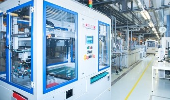
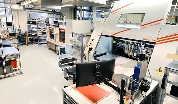
State-of-the-art manufacturing and inspection systems, a high level of automation plus a flexible manufacturing processes allow to produce circuit boards with the highest possible connection density.
Manufacturing processes at DYCONEX are completely integrated into a manufacturing execution system (MES). Materials and processes are 100 percent traceable. The company is ISO 9001, ISO 13485 and EN 9100 certified.
DYCONEX is located in Bassersdorf, roughly 10 minutes from the Zurich/Kloten airport. The firm has total floor space of more than 6'000 m2, of which 600 m2 are a Class 10'000 cleanroom. The company currently has approximately 190 employees.
|
Experience |
Since 1964 (Management buy-out as DYCONEX in 1991) |
|
Headquarters |
Bassersdorf / Zurich, Switzerland |
|
Business premises |
6'000m2, including 600m2 of clean room |
|
Employees |
>190 |
|
Products |
|
|
Main export markets |
USA, Europe, Asia-Pacific, Australia |
|
Management |
Dr. Hubert Zimmermann, Christian Ahr, Bernhard Schmucki, Christian Beck, Dr. Selçuk Mentese |
|
Quality standards |
|
|
Memberships |
EIPC, FED, IMAPS, IPC, MEPTEC, SMTA, Swiss Aerospace Cluster, SWISS MEDTECH, Switzerland Global Enterprise, ZVEI |
|
Financial rating |
Risk Indicator 1 award by Bisnode Dun & Bradstreet for financial stability and high credit standing
|

DYCONEX AG
Grindelstrasse 40
CH-8303 Bassersdorf
Switzerland
Tel. +41 (43) 266 1100
Fax +41 (43) 266 1101
mail.dyconex(at)mst.com
A comprehensive offering goes beyond producing and delivering PCBs. Close cooperation with our customers from the early R&D phase until the product phase-out ensures the best PCB solution: technically as well as financially. This is why DYCONEX offers comprehensive engineering services that accompany customers throughout the product life cycle.
Design & layout
- Feasibility study support
- Consulting on design for manufacturing (build-ups, materials, test procedures)
- CTE control
- Form factor and weight optimization
- Consulting on design for reliability
- Cost optimization support
- Data conversion to Gerber files
- Technical training and workshops
Production & logistics
- Hand carry
- Express shipments
- Buffer stock
- Consignment stock
- Blister packs
Prototyping
- Engineering support
- Fast prototyping services
- Technological prototyping services
- Wrap-up on first prototype run
Years of experience working in the field of life-sustaining medical devices and high-end industrial projects have led to an uncompromising quality management system. The goal is to assure predictability in the manufacture of high-complexity interconnect solutions.
To meet this challenge, DYCONEX has developed an integrated control and inspection concept (DYCO IC2), allowing to continuously improve the business and production processes.
Quality Tools
The implementation of advanced quality tools and techniques provides accountability and is an essential ingredient in the effort for sustainable improvement.
- 100% traceability for every single PCB
- First article inspection
- 8D reports
- DoE, SPC and MSA
- Six Sigma methodology
- Change management
- IQ/OQ/PQ validation methodology
- CAPA process
- Customized inspection concepts and reports
- Maverick control
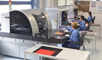
Inspection and Test
Enabled through sophisticated equipment and skilled professionals, the company is determined to supply only high-reliability, Swiss quality solutions to their markets.
- 100% electrical testing
- Automated optical inspection
- Automated final inspection
- Micro-section control
- Interconnect stress test (IST)
- Bondability analysis
- Ionic contamination measurement
- X-ray inspection
- FPC bending tests
- Scanning electron microscope
- TMA/DMA material analysis
Approvals and Standards
DYCONEX’ approvals and quality management system demonstrate the ability to provide PCB solutions that consistently meet applicable customer and regulatory requirements.
- ISO 9001, ISO 13485, EN 9100 and ISO 14001 certified
- Manufacturing and testing according to IPC standards and customer-specific requirements
- Certified Six Sigma Black Belts and IPC qualified employees
- RoHS and REACH compliance
Downloads
|
Ultra-thin base materials take PCB miniaturisation to the next level Flexible and rigid ultra-thin base materials enable highly reliable, thinner PCBs Authors: Daniel Schulze |
|
Flexible Substrates for Smart Sensor Applications A novel approach that delivers miniaturized, hermetic, biostable and highly reliable smart sensor modules. Authors: Dr. Eckardt Bihler, Dr. Marc Hauer, Birgit Neubauer |
|
Why Predictability Matters in High-End PCB Manufacturing An advanced approach that delivers predictability, serving as the basis for assuring ongoing reliability. |
|
Noble Metal PCB Manufacturing for Direct Implants The market of active implantable devices requires new strategies in designing and manufacturing the relevant components. |
DYCONEX AG
Grindelstrasse 40
CH-8303 Bassersdorf
Switzerland
Tel. +41 (43) 266 1100
Fax +41 (43) 266 1101
mail.dyconex(at)mst.com
OUR HISTORY
DYCONEX from 1991 to Today
DYCONEX is proud of its 30-year history and consistent development of leadinge-edge innovations. Our commitment to be the world’s leading provider of complex, ultra dense and highly reliable interconnect solutions has made us what we are today.
Dyconex AG decides to update all wet chemical equipment to the latest leading-edge technology.
- The new “vacuum”-etching process provides unprecedentedly fine subtractive structures, pushing the lines/spaces down to 15 µm with conventional subtractive technology.
- The new equipment also provides a capacity increase of almost double.
Introduction of Hot-E-Test (full electrical test at elevated temperature) to further boost the reliability of our substrates for implantable applications:
- Patented heating frame to heat substrates above 110°C to identify via-related issues on substrates.
- No test coupons – Hot-E-Test performed on usable substrates.
- Standard E-Test and Hot-E-Test can be performed in parallel, providing top reliablity at lower costs.
- Thorough and readily reproducible testing of PCBs is the goal of the automated final inspection newly introduced by Dyconex.
- Automated final inspection is ideal for high production volumes, complex and highly repetitive PCB structures and products with the highest reliability requirements, such as life-supporting medical technology.
- Thanks to the semi-transparent materials that Dyconex uses, automated inspection provides also an image of a PCB’s inner layers.
Dyconex decides to enter into additive and biocompatible interconnect manufacturing by purchasing leading-edge sputter equipment:
- The leading-edge sputtering equipment is to maintain Dyconex’s place on the technological leader board in advanced printed circuits.
- The machine enables the coating of a wide range of thin-film materials which can be structured by the usual lift-off and etching techniques.
- Dyconex awarded EN 9100:2009 aviation and aerospace certification and is added to the OASIS (Online Aerospace Supplier Information System) database.
- With ISO 9001 (1993) and ISO 13485 certification (2012), Dyconex has an extensive QMS guaranteeing superb product reliability and 100% traceability. EN 9100 confirms that Dyconex meets the demanding requirements of the aviation and aerospace industry.
- Increases productivity in production through the targeted use of robot handling systems for loading and unloading laser machines.
- Three specialized robots relieve laser machine operators of repetitive tasks.
- The handling systems enable continuous production by operating both during shift hours and overnight without personnel present.
- The AGV system’s primary task is to transport materials between departments.
- The AGV system enables completely autonomous transport from shelf to shelf. Adapted to Dyconex’s requirements and navigate by themselves, the robots are aided by a laser scanner. They react to changes in the working environment, avoiding people and obstacles on their own.
Dyconex AG makes a major investment in the MXY2 drilling and routing machine from Schmoll Maschinen GmbH. The machine offers:
- Smaller structures and compliance with specific requirements for even higher accuracy.
- Contact depth drilling and optical registration for highly precise machining results
- An included CCD camera allows corrections such as offset, rotation, shrinking, and stretching.
- Further expanding its Reliability Center of Competence and the corresponding IST testing, Dyconex AG puts its fourth IST (interconnect stress test) testing machine into service.
- Dyconex develops extensive and systematic methodologies that make it possible to gather solid evidence about product reliability, using this benefit for critical applications in Medtech or aerospace & aviation.
- Dyconex AG opens new reliability testing lab to serve as a Center of Competence.
- The lab has stations for electrical fault location, thermography and multiple IST (interconnect stress test) units, bending testers , and a scanning electron microscope and optical microscopes for analysis.
- For critical applications, e.g. medical implants, the lab develops models that enable precise conclusions about product reliability using accelerated test procedures.
- The Multibond is applied to high-reliability multilayer PCBs to improve the bonding between the single layers of a board. The underlying principle is a micro-roughening process in combination with an organic copper conversion coating for PCB inner layers.
- The new treatment leads to an improved adhesion between them an the prepregs, thus enhances the peel strenghts of the whole circuit board.
- The Gemstone generation provides small and reliable vias at an unprecedent speed.
- The UV laser is equipped with a very specific galvano-optical laser beam adjustment to significantly increase speed.

- The Gemstone generation provides small and reliable vias at an unprecedent speed.
- The UV laser is equipped with a very specific galvano-optical laser beam adjustment to significantly increase speed.
- The Orbotech ParagonTM-9800 Laser Direct Imaging (LDI) system is a step in converting all exposure jobs to direct imaging. It results in a faster and easier process flow. The system guarantees high throughput for LDI optimized solder masks and other solder mask materials.
- For high-reliability applications such as medtech implants, full traceability is guaranteed with serial number and date stamps and 1D or 2D barcodes for recording process parameters.
- Dyconex awarded ISO 13485:2003 certification, a complement to the ISO 9001 QMS the company has had for many years, proof that Dyconex supplies high-quality and reliability components to the medical market.
- Certification requires evidence of the ability to consistently fulfill customer and regulatory requirements.
- Dyconex invests in CO2/UV combi laser to increase throughput for HDI PCBs and improve blind via quality in rigid glass fiber materials.
- This boosts productivity in blind via formation for rigid substrates, which is faster compared to UV laser drilling.
- Quality improvements due to the selective ablation rates of the two laser systems.
In terms of miniaturization, Dyconex implements a via filling process for mechanical and laser-drilled blind vias. This allows for plate blind vias with an excellent via filling ratio and through holes with stacked blind vias, enabling the shortest signal path.

In terms of miniaturization, Dyconex implements a via filling process for mechanical and laser-drilled blind vias. This allows for plate blind vias with an excellent via filling ratio and through holes with stacked blind vias, enabling the shortest signal path.
- To respond to increasing demands for finer features and denser designs in multilayer PCBs, Dyconex engineers a state-of-the-art registration workflow.
- This improves layer to layer alignment and enables higher process robustness and better product quality and reliability.

- To respond to increasing demands for finer features and denser designs in multilayer PCBs, Dyconex engineers a state-of-the-art registration workflow.
- This improves layer to layer alignment and enables higher process robustness and better product quality and reliability.
- Dyconex enhances its laser debris cleaning capabilities with new plasma desmearing equipment.
- Advancing mechanical drilling, Dyconex implements new, state-of-the art drilling systems capable of producing mechanical holes of 100 µm ⌀ and even 75 µm ⌀ for specialty applications.

- Dyconex enhances its laser debris cleaning capabilities with new plasma desmearing equipment.
- Advancing mechanical drilling, Dyconex implements new, state-of-the art drilling systems capable of producing mechanical holes of 100 µm ⌀ and even 75 µm ⌀ for specialty applications.
- Dyconex becomes a part of the MST Group, comprised of four international technology companies.
- Dyconex AG’s innovations are an asset for MST. Miniaturized electronic modules are set to become important in the fast-growing medical markets.

- Dyconex becomes a part of the MST Group, comprised of four international technology companies.
- Dyconex AG’s innovations are an asset for MST. Miniaturized electronic modules are set to become important in the fast-growing medical markets.
- Dyconex AG begins investigating molded interconnect device (MID) targeting applications in the medical and defense markets. The stable 3D form complements flexible PCBs for low- to mid-complexity interconnects with high 3D-alignment precision requirements.
- First uses of low-cost injection-molded LCP antenna horn with metallization to replace high-cost traditional metal brass-routed HF components.
- After 1.5 years of development, Dyconex releases new in-house PCB engineering software. The application, "Prisma", defines stack-ups, operation plans, and process parameters of PCBs. It produces quotes and manufacturing documents.
- Prisma is the new iteration of the old engineering software (TEDA).
- LCP-based microwave circuit for 60 - 94 GHz mm-wave scanner.
- Active low-noise amplifier (LNA) and detector diodes are integrated via laser-ablated cavities into the LCP substrate.
- Low-cost injection-molded LCP antenna horn with metallization to replace high-cost traditional meta-routed HF components.
- A technology is developed based on printed circuit manufacturing technologies, enabling volume production of polymer microfluidic substrates with integrated microelectrodes for a range of biomedical applications.

- A technology is developed based on printed circuit manufacturing technologies, enabling volume production of polymer microfluidic substrates with integrated microelectrodes for a range of biomedical applications.
- To support its fast-growing US customer base even better, Dyconex AG decides to set up a sales and application engineering office in Phoenix AR.
- Providing local application engineering, especially for flex PCBs to help make more customers aware of the flex technology so they can improve PCB reliability and further miniaturize electronic modules.
- As an alternative to in-situ deposited thin film or thick film passive components, DYCONEX developed an integration technology based on embedding discrete ultra flat high precision resistors within flexible multi-layer substrates.
- The resulting flexible printed circuit boards were evaluated according to basic electrical, mechanical and thermal testing procedures (IPC/JEDEC) and displayed excellent robustness.
- Development of the liquid crystal polymer (LCP) lamination process to manufacture LCP multilayer and microvia boards (2 and 4 layers) for millimeter wave-phased array antennas.
- Growing business in the US market for medical implantable applications, defibrillators, and pacemakers. (Guidant)

- Development of the liquid crystal polymer (LCP) lamination process to manufacture LCP multilayer and microvia boards (2 and 4 layers) for millimeter wave-phased array antennas.
- Growing business in the US market for medical implantable applications, defibrillators, and pacemakers. (Guidant)
- New equipment to increase miniaturization and HDI reliability by plasma/laser via combination.
- New depth routing in flexible multilayers for better bending. Extension of sensor fields applications.

- New equipment to increase miniaturization and HDI reliability by plasma/laser via combination.
- New depth routing in flexible multilayers for better bending. Extension of sensor fields applications.
- Company relocation from Seebach to a new production site in Bassersdorf.
- CAPEX of over CHF 10 million for new, cutting-edge equipment.
- All processes for flexible substrate manufacturing (as DYCOstrate®) are optimized using the increased production floor space.
- Significant increase in production capacity and major improvements in process stability, sales growth and personnel expansion.
- Sharp increase in orders from the field of audiology/medical devices with microvia technology. Increased complexity with 2x5-layer DYCOstrate® build-up for military defence applications and satellites.
- Development of BGA interposer technology (DYCOre®) for complex fanout designs.
- Wraparound microvia build-up for high-end application (flex with metal core, high heat dissipation).
- Transition from conventional, rigid/rigidly flexible circuit board technologies (Denstrate®, Constrate®, Dycoflex®) to DYCOstrate® microvia plasma technology for mass production in the medical field. Plasma etching technology is superior to mechanical drilling in cost, speed, and size.
- Sequential flex build-up is used to increase artwork alignment of neighboring layers to drive miniaturization.
- DYCOstrate® trademark registered in Switzerland. License agreements with HP, IBM, and Würth Electronic for DYCOstrate® via technology.
- Dycostrate substrate combines high density interconnects (HDIs) with thermal and mechanical elements suited to harsh environments.
- A thin, flexible substrate, treated using plasma via technology, is used for the electrical connections. Thermal vias can be added for high thermal conductivity.
- A rigid core gives mechanical stability and thermal dissipation and can be made from conductive material.
- The printed circuit board (PCB) division of Contraves was born in 1964.
- Foundation as Dyconex of the Contraves PCB division. Dyconex pioneers PCB manufacturing, reaching key technological milestones, beginning with the introduction of high-reliability, rigid-flex multilayer boards (DYCOflex®).
- Contraves started its PCB activities in 1964. Its PCB division is active in R&D and in defence applications. Plasma etching vias (instead of mechanical drilling) is a cornerstone of Dyconex.
Dyconex AG decides to update all wet chemical equipment to the latest leading-edge technology.
- The new “vacuum”-etching process provides unprecedentedly fine subtractive structures, pushing the lines/spaces down to 15 µm with conventional subtractive technology.
- The new equipment also provides a capacity increase of almost double.
Introduction of Hot-E-Test (full electrical test at elevated temperature) to further boost the reliability of our substrates for implantable applications:
- Patented heating frame to heat substrates above 110°C to identify via-related issues on substrates.
- No test coupons – Hot-E-Test performed on usable substrates.
- Standard E-Test and Hot-E-Test can be performed in parallel, providing top reliablity at lower costs.
- Thorough and readily reproducible testing of PCBs is the goal of the automated final inspection newly introduced by Dyconex.
- Automated final inspection is ideal for high production volumes, complex and highly repetitive PCB structures and products with the highest reliability requirements, such as life-supporting medical technology.
- Thanks to the semi-transparent materials that Dyconex uses, automated inspection provides also an image of a PCB’s inner layers.
Dyconex decides to enter into additive and biocompatible interconnect manufacturing by purchasing leading-edge sputter equipment:
- The leading-edge sputtering equipment is to maintain Dyconex’s place on the technological leader board in advanced printed circuits.
- The machine enables the coating of a wide range of thin-film materials which can be structured by the usual lift-off and etching techniques.
- Dyconex awarded EN 9100:2009 aviation and aerospace certification and is added to the OASIS (Online Aerospace Supplier Information System) database.
- With ISO 9001 (1993) and ISO 13485 certification (2012), Dyconex has an extensive QMS guaranteeing superb product reliability and 100% traceability. EN 9100 confirms that Dyconex meets the demanding requirements of the aviation and aerospace industry.
- Increases productivity in production through the targeted use of robot handling systems for loading and unloading laser machines.
- Three specialized robots relieve laser machine operators of repetitive tasks.
- The handling systems enable continuous production by operating both during shift hours and overnight without personnel present.
- The AGV system’s primary task is to transport materials between departments.
- The AGV system enables completely autonomous transport from shelf to shelf. Adapted to Dyconex’s requirements and navigate by themselves, the robots are aided by a laser scanner. They react to changes in the working environment, avoiding people and obstacles on their own.
Dyconex AG makes a major investment in the MXY2 drilling and routing machine from Schmoll Maschinen GmbH. The machine offers:
- Smaller structures and compliance with specific requirements for even higher accuracy.
- Contact depth drilling and optical registration for highly precise machining results
- An included CCD camera allows corrections such as offset, rotation, shrinking, and stretching.
- Further expanding its Reliability Center of Competence and the corresponding IST testing, Dyconex AG puts its fourth IST (interconnect stress test) testing machine into service.
- Dyconex develops extensive and systematic methodologies that make it possible to gather solid evidence about product reliability, using this benefit for critical applications in Medtech or aerospace & aviation.
- Dyconex AG opens new reliability testing lab to serve as a Center of Competence.
- The lab has stations for electrical fault location, thermography and multiple IST (interconnect stress test) units, bending testers , and a scanning electron microscope and optical microscopes for analysis.
- For critical applications, e.g. medical implants, the lab develops models that enable precise conclusions about product reliability using accelerated test procedures.
- The Multibond is applied to high-reliability multilayer PCBs to improve the bonding between the single layers of a board. The underlying principle is a micro-roughening process in combination with an organic copper conversion coating for PCB inner layers.
- The new treatment leads to an improved adhesion between them an the prepregs, thus enhances the peel strenghts of the whole circuit board.
- The Gemstone generation provides small and reliable vias at an unprecedent speed.
- The UV laser is equipped with a very specific galvano-optical laser beam adjustment to significantly increase speed.
- The Orbotech ParagonTM-9800 Laser Direct Imaging (LDI) system is a step in converting all exposure jobs to direct imaging. It results in a faster and easier process flow. The system guarantees high throughput for LDI optimized solder masks and other solder mask materials.
- For high-reliability applications such as medtech implants, full traceability is guaranteed with serial number and date stamps and 1D or 2D barcodes for recording process parameters.
- Dyconex awarded ISO 13485:2003 certification, a complement to the ISO 9001 QMS the company has had for many years, proof that Dyconex supplies high-quality and reliability components to the medical market.
- Certification requires evidence of the ability to consistently fulfill customer and regulatory requirements.
- Dyconex invests in CO2/UV combi laser to increase throughput for HDI PCBs and improve blind via quality in rigid glass fiber materials.
- This boosts productivity in blind via formation for rigid substrates, which is faster compared to UV laser drilling.
- Quality improvements due to the selective ablation rates of the two laser systems.
In terms of miniaturization, Dyconex implements a via filling process for mechanical and laser-drilled blind vias. This allows for plate blind vias with an excellent via filling ratio and through holes with stacked blind vias, enabling the shortest signal path.
- To respond to increasing demands for finer features and denser designs in multilayer PCBs, Dyconex engineers a state-of-the-art registration workflow.
- This improves layer to layer alignment and enables higher process robustness and better product quality and reliability.
- Dyconex enhances its laser debris cleaning capabilities with new plasma desmearing equipment.
- Advancing mechanical drilling, Dyconex implements new, state-of-the art drilling systems capable of producing mechanical holes of 100 µm ⌀ and even 75 µm ⌀ for specialty applications.
- Dyconex becomes a part of the MST Group, comprised of four international technology companies.
- Dyconex AG’s innovations are an asset for MST. Miniaturized electronic modules are set to become important in the fast-growing medical markets.
- Dyconex AG begins investigating molded interconnect device (MID) targeting applications in the medical and defense markets. The stable 3D form complements flexible PCBs for low- to mid-complexity interconnects with high 3D-alignment precision requirements.
- First uses of low-cost injection-molded LCP antenna horn with metallization to replace high-cost traditional metal brass-routed HF components.
- After 1.5 years of development, Dyconex releases new in-house PCB engineering software. The application, "Prisma", defines stack-ups, operation plans, and process parameters of PCBs. It produces quotes and manufacturing documents.
- Prisma is the new iteration of the old engineering software (TEDA).
- LCP-based microwave circuit for 60 - 94 GHz mm-wave scanner.
- Active low-noise amplifier (LNA) and detector diodes are integrated via laser-ablated cavities into the LCP substrate.
- Low-cost injection-molded LCP antenna horn with metallization to replace high-cost traditional meta-routed HF components.
- A technology is developed based on printed circuit manufacturing technologies, enabling volume production of polymer microfluidic substrates with integrated microelectrodes for a range of biomedical applications.
- To support its fast-growing US customer base even better, Dyconex AG decides to set up a sales and application engineering office in Phoenix AR.
- Providing local application engineering, especially for flex PCBs to help make more customers aware of the flex technology so they can improve PCB reliability and further miniaturize electronic modules.
- As an alternative to in-situ deposited thin film or thick film passive components, DYCONEX developed an integration technology based on embedding discrete ultra flat high precision resistors within flexible multi-layer substrates.
- The resulting flexible printed circuit boards were evaluated according to basic electrical, mechanical and thermal testing procedures (IPC/JEDEC) and displayed excellent robustness.
- Development of the liquid crystal polymer (LCP) lamination process to manufacture LCP multilayer and microvia boards (2 and 4 layers) for millimeter wave-phased array antennas.
- Growing business in the US market for medical implantable applications, defibrillators, and pacemakers. (Guidant)
- New equipment to increase miniaturization and HDI reliability by plasma/laser via combination.
- New depth routing in flexible multilayers for better bending. Extension of sensor fields applications.
- Company relocation from Seebach to a new production site in Bassersdorf.
- CAPEX of over CHF 10 million for new, cutting-edge equipment.
- All processes for flexible substrate manufacturing (as DYCOstrate®) are optimized using the increased production floor space.
- Significant increase in production capacity and major improvements in process stability, sales growth and personnel expansion.
- Sharp increase in orders from the field of audiology/medical devices with microvia technology. Increased complexity with 2x5-layer DYCOstrate® build-up for military defence applications and satellites.
- Development of BGA interposer technology (DYCOre®) for complex fanout designs.
- Wraparound microvia build-up for high-end application (flex with metal core, high heat dissipation).
- Transition from conventional, rigid/rigidly flexible circuit board technologies (Denstrate®, Constrate®, Dycoflex®) to DYCOstrate® microvia plasma technology for mass production in the medical field. Plasma etching technology is superior to mechanical drilling in cost, speed, and size.
- Sequential flex build-up is used to increase artwork alignment of neighboring layers to drive miniaturization.
- DYCOstrate® trademark registered in Switzerland. License agreements with HP, IBM, and Würth Electronic for DYCOstrate® via technology.
- Dycostrate substrate combines high density interconnects (HDIs) with thermal and mechanical elements suited to harsh environments.
- A thin, flexible substrate, treated using plasma via technology, is used for the electrical connections. Thermal vias can be added for high thermal conductivity.
- A rigid core gives mechanical stability and thermal dissipation and can be made from conductive material.
- The printed circuit board (PCB) division of Contraves was born in 1964.
- Foundation as Dyconex of the Contraves PCB division. Dyconex pioneers PCB manufacturing, reaching key technological milestones, beginning with the introduction of high-reliability, rigid-flex multilayer boards (DYCOflex®).
- Contraves started its PCB activities in 1964. Its PCB division is active in R&D and in defence applications. Plasma etching vias (instead of mechanical drilling) is a cornerstone of Dyconex.

DYCONEX AG
Grindelstrasse 40
CH-8303 Bassersdorf
Switzerland
Tel. +41 (43) 266 1100
Fax +41 (43) 266 1101
mail.dyconex(at)mst.com