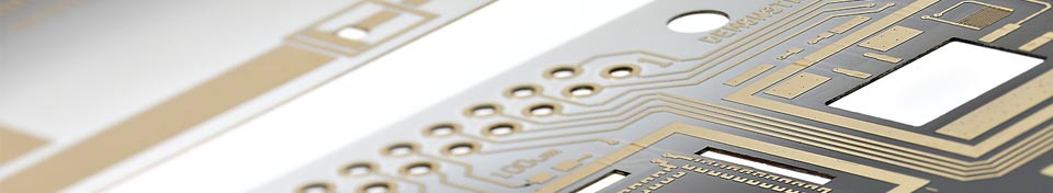
LCP - Liquid Crystal Polymer
Liquid Crystal Polymer (LCP) is a thermoplastic polymer material with unique structural and physical properties. It demonstrates simultaneously exceptional performance with respect to electrical, thermal, mechanical and chemical properties. LCP is the perfect match for technically demanding high frequency, harsh environment and direct implantable applications. Due to its thermoplastic characteristics it can be thermoformed – even as a complex multilayer flex with embedded thin film traces – to various shapes.
Remaining steadfast in its commitment to make the exceptional advantages of LCP available to the industry, DYCONEX has successfully developed and established viable volume production manufacturing processes and has acquired unmatched experience, competence and expertise in LCP applications since many years.
Technology highlights
For high frequency applications
- Superior dielectric characteristics enabling high-frequency applications up to 110 GHz
- Combination of high-Tg LCP with high Tg LCP bondply or low-Tg LCP adhesive for high multi-layer build-ups up to 10 layers
- Cost-competitive high-frequency FPC technology (relative to PTFE)
- Mixed-material combinations (LCP-Polyimide or LCP-BT-Epoxy)
- Thin film vacuum coating of special materials for sensor functionalities
General capabilities for LCP flex circuit boards:
For biomedical applications
- Fully biocompatible according to ISO 10993-5 (in vitro cytotoxicity)
- Adhesiveless multilayer build-ups resulting in homogeneous structures up to 4-layer
- Thin film vacuum coating of noble metals
For all applications
- Applicable for Ultra-HDI structuring supported by thin film technology
- Light-weight with high flexural endurance
- Low moisture absorption and low moisture permeability (near-hermetic)
- 3D forming to various shapes
- Special features: cavities, fold-lines, thinned bending zones
- Ultra-fine line flex cables
|
Description |
Standard capabilites |
|
Lines/spaces |
25/35µm |
|
Microvias/pads diameter (laser) |
50/250 µm |
|
Thinnest starting material |
25 µm |
|
Thinnest dielectric thickness |
25 µm |
|
Conductor width tolerance |
+/- 20% |
|
Artwork to soldermask tolerance |
+/- 25 µm |
|
Layer count |
4 |
|
Description |
Leading-edge capabilities |
|
Lines/spaces |
20/25 µm |
|
Microvias/pads diameter (laser) |
400/200µm |
|
Thinnest starting material |
25 µm |
|
Thinnest dielectric thickness |
25 µm |
|
Conductor width tolerance |
+/- 10% |
|
Artwork to soldermask tolerance |
+/- 15 µm |
|
Layer count |
6-8 |
|
Min. PCB thickness |
|
|
2 layers |
25 µm |
|
3 layers |
75 µm |
|
Up tp 8 layers |
325 µm |