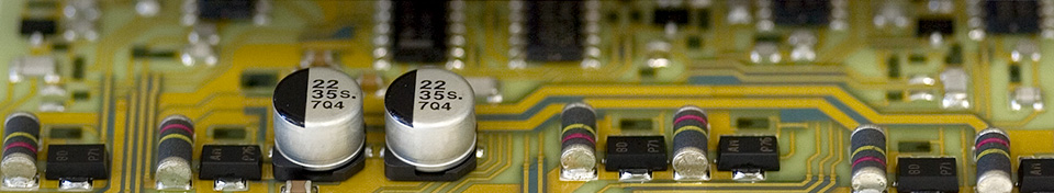
Thick film
Standard thick film ceramic (96% alumina) substrates are engineered to minimize as-fired resistor variations and maximize aged adhesion values. Superior resistor stability is achieved by controlling the substrates' effects on the temperature coefficient of resistance.
The standard thick film ceramic substrate is particularly well suited for small geometry, high resistor value circuitry.
Thick film process flow
Thick film features
Substrate properties
After scribing / drilling with a CO2 laser and a cleaning step the alumina substrates are patterned by screen printing, followed by a drying and the final sintering step.
Thick film features and thick film properties
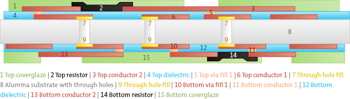
Thick film circuits are available in a variety of layer structures from single sided with single layer to multilayer on two sides. The thick film multilayer structure allows for up to three layers on both sides.
Quality performance testing and assurance
In-process and final inspection procedures include:
- Electrical test using flying probe test system
- Visual inspection
- Customer requirements according specification
Thick film dimensional capabilities
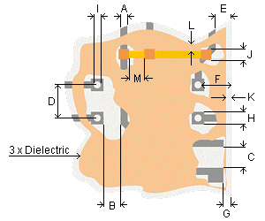
|
Index |
Description |
Standard |
Leading edge |
|
H |
Coverpad through hole |
500 µm |
400 µm |
|
I |
Through hole diameter |
200 µm |
150 µm |
|
J |
Via pad |
400 µm |
300 µm |
|
K |
Dielectric to substrate edge |
200 µm |
200 µm |
|
L |
Conductor to dielectric edge |
200 µm |
200 µm |
|
M |
Via pitch at same potential |
≥ 0 µm |
≥ 0 µm |
|
Index |
Description |
Standard |
Leading edge |
|
A |
Line width |
200 µm |
100 µm |
|
B |
Line to via coverpad spacing |
200 µm |
150 µm |
|
C |
Line spacing |
200 µm |
100 µm |
|
D |
Through hole pitch |
800 µm |
700 µm |
|
E |
Line to edge spacing |
250 µm |
200 µm |
|
F |
Via to edge spacing |
400 µm |
400 µm |
|
G |
Pad to edge spacing |
300 µm |
200 µm |
Aluminum oxide substrate properties
|
Material |
96% Al2O3 |
|
Color |
white |
|
Maximum substrate size |
4" x 6" |
|
TCE (10E+6/°C) |
6.8 |
|
Thermal conductivity (W/mK) |
24 |
|
Dielectric strength (kV/mil) |
>1° |
|
Dielectric constant (relative permitivity) 1 MHz |
9.8 |
|
Dissipation factor (loss tangent) 1 MHz |
0.00034 |
Available conductor material composition
- Au
- PtPdAu
- PtAu
- Ag
- AgPd
Thick film resistor range: available from 10Ω - 10MΩ pastes