Micro Systems Engineering GmbH (MSE)
Profile
Facts & Figures
Engineering
Quality
Publications
Since 1984 MSE has specialized in customer-specific solutions for advanced microelectronics. The company belongs to the leading European suppliers of complex LTCC (Low Temperature Co-fired Ceramics) substrates, advanced board assembly and semiconductor packaging technologies.
From the early days until now, the manufacture of electronic modules for implantable active devices at the highest quality level has been one of main business segments. MSE has focused on excellence ever since.
Further, MSE has always been convinced that all the knowledge, experience and dedication mandatory in medical device production should also be available to customers of other industries who likewise expect leading-edge production technology. The company applies the expertise and experience it has gained in medical technology to every sector where high reliability, miniaturization, high temperatures, high frequencies or hermetic encapsulation play an important role.
MSE supports its customers as a partner from the concept phase through prototyping to volume production, from design support through quality management to procurement.
Based on customer-specific requirements, MSE offers all the key processes needed to manufacture an electronic module from one source:
- Design service for ceramic and organic substrates, as well as others such as thin film, DCB, etc.
- Substrate manufacturing: LTCC (low-temperature co-fired ceramics) and thick film
- Advanced assembly processes such as SMT, flip chip, wire bonding, die attach, etc. on any base materials
- Packaging processes for BGA (ball grid arrays), LGA (land grid arrays), QFP (quad flat packages), etc.
- Special services including customer-specific tests, project management, validation, materials procurement on a worldwide basis, etc.
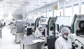
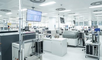
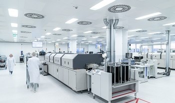
The most modern production lines, comprehensive test and inspection equipment, 100 percent traceability for processes and materials guarantee top-level solutions in microelectronics.
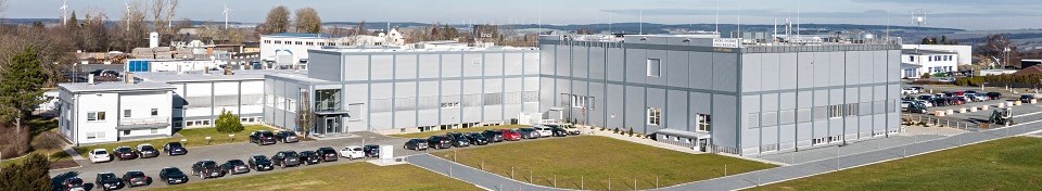
With some 300 skilled workers, technicians, engineers and scientists MSE has the critical mass for all key processes, still maintaining the efficiency and flexibility of a mid-sized enterprise. MSE has its headquarters in Berg (Upper Franconia), roughly 60 km north of Bayreuth, Germany. The facility located there has a total floor space of 6’000 m2. MSE is ISO 13485, ISO 9001 and ISO 50001 certified.

Micro Systems Engineering GmbH
Schlegelweg 17
DE-95180 Berg
Germany
Tel. +49 (9293) 78-0
Fax +49 (9293) 78-41
info.msegmbh(at)mst.com
|
Foundation |
1984 |
|
Headquarters |
D-95180 Berg (Northern Bavaria), Germany |
|
Business premises |
6000 m2, including 2500 m2 clean room |
|
Employees |
300 |
|
Products & services |
|
|
Main export markets |
Europe, USA |
|
Management |
Thomas Asperger |
|
Quality standards |
|
|
Memberships |
Cluster Mikrosystemtechnik, iMAPS Germany, iMAPS International, INNOMAG, DVS, MEPTEC, SMTA |
Micro Systems Engineering GmbH
Schlegelweg 17
DE-95180 Berg
Germany
Tel. +49 (9293) 78-0
Fax +49 (9293) 78-41
info.msegmbh(at)mst.com
Design services
MSE offers concepts and design support for the following technologies:
- LTCC (substrates manufactured by MSE)
- Thick film (substrates manufactured by MSE)
- HTCC (High Temperature Co-fired Ceramic)
- HDI PCB (High Density Interconnect Printed Circuit Board)
- Rigid-flex PCB
- DCB (Direct Bonded Copper)
- Thin film
- MCM (Multi Chip Modules)
- SiP (System in Package)
The MSE team works with the following design systems and interfaces:
- Altium Designer
- CAM 350
- Gerber + aperture table
- Extended Gerber preferred
- DXF
- HPGL
- Graffy/Hyde
R&D projects
MSE is participating in various government funded research and development projects to maintain its leading position in the electronics world.
In addition to other projects, MSE is currently working on:
|
BiSWind |
Miniaturized and energy autonomous sensor elements based on complex 3D-shaped LTCC substrates to facilitate real time supervision of wind turbine shaft systems |
|
MultiMat |
Multi material systems for enhanced sensor integration and miniaturization based onceramic substrates by additive manufacturing processes |
|
MecDruForm |
Plastic films by combining printing technologies |
MSE was founded as a supplier of electronic modules for implantable pacemakers. The development and manufacture of modules for life-sustaining medical devices and other critical applications characterise the quality awareness and the management system of MSE.
Every employee's activities are highly focused on customer requirements plus the quality and reliability of all products and services.Continual improvement of all processes, ongoing training and further education as well as the careful and efficient use of all resources are further cornerstones of MSE's uncompromising quality policy.
During manufacturing, MSE guarantees complete traceability of materials and processes. A wide range of manufacturing tests, stress tests and other means of analysis is available to demonstrate the performance of components and modules.
Today, the effectiveness of MSE's quality system is confirmed by official certification to ISO 13485, ISO 9001 and ISO 50001.
Inspection and Test
- X-Ray and CT
- 01005 and fine-pitch inspection
- Combined 2D / 3D CT-operation
- Solder joint analysis
- Package inspection - Scanning Acoustic Microscopy
- Detection of delamination, cracks, voids and porosity - Optical surface scan
- Cross sectioning
- Temperature cycling (-65°C/+250°C)
- Hermeticity test
- Wire pull test
- Component shear test
- Flying probe tester
- Contamination measurement
- X-ray fluorescence method
- SEM/EDX (external service)
Downloads
MSE has published a wide range of papers in the field of ceramic circuits and in the field of assembly and packaging. If you are interested in receiving the full paper please contact MSE under following e-mail address: info.msegmbh(at)mst.com.
Publications in the field of assembly and packaging
|
Miniaturization for Implants and Other Medical Products Employing Ultra-Fine Pitch Flip Chip Technology Dohle, R., Goßler, J., Friedrich, T., Wirth, A., Gorywoda, M., |
|
Small Form-Factor, Liquid-Cooled SiuPM Module for PET/MRI Applications Dohle, R., Rittweg, T., Sacco, I., |
|
New Assembly Technology for VCSEL Arrays Comprising Ultra-Thin Diodes Dohle, R., Friedrich, T., Guo, J, Goßler, J., |
|
Advanced Packaging Technology for Novel 1-dimensional and 2-dimensional VCSEL Arrays Dohle, R., Henning, G., Wallrodt, M., Greus, G., Neumeyr, C., |
|
New Packaging Technology for Disruptive 1- and 2-Dimensional VCSEL Arrays and Their Electro-Optical Performance and Applications Dohle, R., Henning, G., Friedrich, T., Wallrodt, M., Greus, G., Neumeyr, C., Rosskopf, J., Kemeter, M., |
|
New Packaging Technology for 2-dimensional VCSEL Arrays and Their Electro-Optical Performance and Applications Dohle, R., Friedrich, T., Henning, G., Wallrodt, M., Greus, C., Rosskopf, J., Hohenleitner, R., Neumeyr, C., |
|
LTCC-Based Highly Integrated SiPM Module With Integrated Liquid Cooling Channels for High Resolution Molecular Imaging R. Dohle, I. Sacco, Th. Rittweg, Th. Friedrich, G. Henning, J. Goßler, P. Fischer, |
|
Study on electromigration in flip chip lead-free solder connections with 40 µm or 30 µm diameter on thin film ceramic substrates Gorywoda M., Dohle R., Kandler B., Burger B., |
|
On the failure mechanism in lead-free flip-chip interconnects comprising ENIG finish during electromigration Dohle, R., Gorywoda, M., Wirth, A., Burger, B., Goßler, J., |
|
Investigation of electromigration behaviour in lead-free flip-chip solder connections Dohle, R., Gorywoda, M., Wirth, A., Goßler, J., |
|
Small to Mid Quantity SDBGA Packaging Line for Active Medical Implants: Conception, Implementation and Challenges Perrone, R., Goßler, J., |
|
Langzeitstudie zur Elektromigration in bleifreien Flip Chips mit Lotkugeldurchmessern von 50 µm oder 60 µm und ENIG-Finish auf der Chip- und Leiterplattenseite Marek Gorywoda, Dr. Rainer Dohle, Andreas Wirth, Bernd Burger, Jörg Gossler, |
|
Produktionsprozesse für Stacked Die Ball Grid Arrays Jörg Gossler, |
|
Long-Term Electromigration Study of Lead-Free Flip-Chips with Solder Bumps with 50 µm or 60 µm Diameter Employing ENIG Surface Finish on Both Chip and Substrate Side Gorywoda, M., Dohle, R., Härter, S., Wirth, A., Goßler, J., Franke, J., |
|
Electromigration Performance of Flip-Chips with Lead-Free Solder Bumps between 30 µm and 60 µm Diameter Dohle, R., Härter, S., Wirth, A., Goßler, J. Gorywoda, M., Reinhardt, A., Franke, J., |
|
Reliability Study of Lead-Free Flip-Chips with Solder Bumps Down to 30 µm Diameter Härter, S., Dohle, R., Reinhardt, A., Goßler, J., Franke, J., |
|
Zuverlässigkeit hochminiaturisierter Flip-Chip Baugruppen mit Leiterplatten in Subtraktivtechnologie Dohle, R., Friedrich, T., Goßler, J., Georgiev, G., |
|
Packaging eines Beschleunigungssensors für aktive medizinische Implantate R. Perrone, T.Friedrich und J. Goßler, |
|
Assembly und Packaging von Elektronikmodulen für medizinische Implantate Jörg Goßler, |
|
Accelerated Life Tests of Flip-Chips with Solder Bumps Down to 30 µm Diameter Dohle, R., Härter, S., Goßler, J., Franke, J., |
|
Wafer Level Solder Bumping and Flip Chip Assembly with Solder Balls Down to 30 µm Oppert, T., Dohle, R., Franke, J., Härter, S., |
|
Assembly and Packaging von Elektronikmodulen für medizinische Implantate - ein Überblick R. Perrone, J. Gossler, |
|
Processing and Reliability Analysis of Flip-Chips With Solder Bumps Down to 30 µm Diameter Franke, J., Dohle, R., Schüßler, F., Oppert, T., Friedrich, T., Härter, S., |
|
Solder Bumping and Processing of Flip-Chips with a Solder Bump Diameter of 30 μm or 40 μm Oppert, T., Dohle, R., Schüßler, F., Franke, J., |
|
Room Temperature Wedge-Wedge Ultrasonic Bonding using Aluminum Coated Copper Wire Dohle, R., Petzold, M., Klengel, R., Schulze, H., Rudolf, F., |
|
Kontaktierungsverfahren und Prozesstechnik für Ultra-Fine-Pitch-Baugruppen Autorenkollektiv, |
|
Passive Integration für LTCC Mikrowellen-Module - Technologie und Design Optimierung Rubén Perrone, Jens Müller, |
|
State of the Art of Assembly and Packaging of Electronic Modules for Medical Implants Jörg Goßler, |
|
Adapted Assembly Processes for Flip-Chip Technology With Solder Bumps of 50 µm or 40 µm Diameter Dohle, R., Schüßler, F., Friedrich, T., Goßler, J., Oppert, T., Franke, J., |
|
Automatisierte Bestückung und Underfill von Ultra-Fine-Pitch Flip-Chips Dohle, R., Schüßler, F., Friedrich, T., Goßler, J., Oppert, T., Franke, J., |
|
Hochpolige Fine-Pitch-Ball-Grid-Array-Baugruppen mit niedrigschmelzenden Lotwerkstoffen Dohle, R. Goßler, J., Kemethmüller, S., Pohlner, J., Dünne, T., |
|
Assembly und Packaging von Elektronikmodulen für medizinische Implantate - ein Überblick Jörg Goßler, |
|
Bereitstellung kleinster Lotmengen bei feinsten Anschlussstrukturen Dohle, R., |
|
Flip-Chip-Technologie - fit für künftige Anforderungen ? Jörg Goßler, |
|
Automatisierte Bestückung und Underfill von Ultra-Fine-Pitch Flip-Chips Rainer Dohle, Thomas Friedrich, Jörg Goßler, |
Publications in the field of LTCC and thick film circuits
|
LTCC-Based Highly Integrated SiPM Module With Integrated Liquid Cooling Channels for High Resolution Molecular Imaging R. Dohle, I. Sacco, Th. Rittweg, Th. Friedrich, G. Henning, J. Goßler, P. Fischer, |
|
Embedded Cavity based Dielectric Loss Measurements for LTCC Substrates up to 110 GHz A. Talai, F. Steinhaußer, A. Bittner, U. Schmid, R. Weigel, D. Schwanke, Th. Rittweg, A. Koelpin, |
|
LTCC Based Microfluidic Mass Flow Sensor Concept C. Zeilmann, T. Haas, A. Backes, U. Schmid, |
|
Micro Fluidic Mass Flow Sensor Concept for Functional Ceramic Circuits C. Zeilmann, T. Haas, A. Backes, U. Schmid, |
|
Verbundprojekt AeroSens, Ziele und Struktur des Projektes, Testvehikel-Fertigung durch MSE Dieter Schwanke, Jürgen Pohlner, Cluster AeroSens, |
|
Optimization of silver paste for flexography printing on LTCC substrate R. Faddoul, N. Reverdy-Bruas, A. Blayo, T. Haas, C. Zeilmann, |
|
Investigation of Pressure Sensor Concepts for Functional Ceramic Circuits T. Haas, C. Zeilmann, U. Schmid, |
|
Manufacturing Processes for Pressure Sensors Realized in LTCC T. Haas, C. Zeilmann, U. Schmid, A. Bittner, |
|
Investigation of Innovative Cooling Concepts for Functional Ceramic Circuits T. Haas, C. Zeilmann, A. Backes, A. Bittner, U. Schmid, |
|
Investigation on Micromachining Technologies for the Realization of LTCC Devices and Systems T. Haas, C. Zeilmann, A. Bittner, U. Schmid, |
|
Passive Integration für LTCC-Mikrowellen-Module - Technologie- und Designoptimierung Ruben Perrone, Dieter Schwanke, Jens Müller, |
|
Design and Evaluation of an Active Cooling Concepts for Functional Ceramic Circuits T. Haas, C. Zeilmann, A. Backes, A. Bittner, U. Schmid, |
|
Entwicklung nanotechnologischer Siebbeschichtungen und daran angepasster Pastensysteme für den Fine-Line-Druck von keramischen Schaltungsträgern D. Schwanke et. al., |